- 您现在的位置:买卖IC网 > Sheet目录2004 > LTC1750IFW#PBF (Linear Technology)IC ADC 14BIT 80MSPS SMPL 48TSSOP
16
LTC1750
1750f
Maximum and Minimum Encode Rates
The maximum encode rate for the LTC1750 is 80Msps. For
the ADC to operate properly the encode signal should have
a 50% (
±4%) duty cycle. Each half cycle must have at least
6ns for the ADC internal circuitry to have sufficient settling
time for proper operation. Achieving a precise 50% duty
cycle is easy with differential sinusoidal drive using a
transformer or using symmetric differential logic such as
PECL or LVDS. When using a single-ended encode signal
asymmetric rise and fall times can result in duty cycles that
are far from 50%.
At sample rates slower than 80Msps the duty cycle can
vary from 50% as long as each half cycle is at least 6ns.
The lower limit of the LTC1750 sample rate is determined
by droop of the sample-and-hold circuits. The pipelined
architecture of this ADC relies on storing analog signals on
APPLICATIO S I FOR ATIO
WU
UU
small valued capacitors. Junction leakage will discharge
the capacitors. The specified minimum operating fre-
quency for the LTC1750 is 1Msps.
DIGITAL OUTPUTS
Digital Output Buffers
Figure 9 shows an equivalent circuit for a single output
buffer. Each buffer is powered by OVDD and OGND, iso-
lated from the ADC power and ground. The additional
N-channel transistor in the output driver allows operation
down to low voltages. The internal resistor in series with
the output makes the output appear as 50
to external
circuitry and may eliminate the need for external damping
resistors.
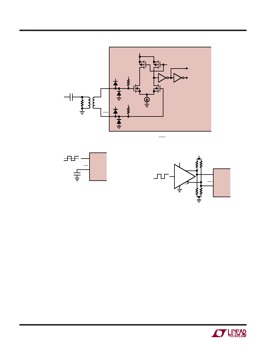
Figure 7. Transformer Driven ENC/ENC
Figure 8a. Single-Ended ENC Drive,
Not Recommended for Low Jitter
Figure 8b. ENC Drive Using a CMOS-to-PECL Translator
VDD
LTC1750
1750 F07
BIAS
VDD
5V
ENC
ANALOG INPUT
2V BIAS
1:4
0.1
F
CLOCK
INPUT
50
6k
TO INTERNAL
ADC CIRCUITS
1750 F08a
ENC
2V
VTHRESHOLD = 2V
ENC
0.1
F
LTC1750
1750 F08b
ENC
130
3.3V
130
D0
Q0
MC100LVELT22
LTC1750
83
83
发布紧急采购,3分钟左右您将得到回复。
相关PDF资料
LTC1799HS5#TRPBF
IC OSC SILICON 33MHZ TSOT23-5
LTC1821ACGW
IC D/A CONV 16BIT PRECISE 36SSOP
LTC1851CFW
IC ADC 12BIT 1.25MSPS 48-TSSOP
LTC1853IFW#TRPBF
IC A/D CONV 8CH 12BIT 48-TSSOP
LTC1856IG#PBF
IC ADC 16BIT 100KSPS 28-SSOP
LTC1859IG#TRPBF
IC A/D CONV 8CH 16BIT 28-SSOP
LTC1867AIGN#TRPBF
IC ADC 16BIT 8CH 200KSPS 16SSOP
LTC1867LCGN#PBF
IC ADC 16BIT 8CH 175KSPS 16SSOP
相关代理商/技术参数
LTC1750IFW#TR
功能描述:IC ADC 14BIT 80MSPS SMPL 48TSSOP RoHS:否 类别:集成电路 (IC) >> 数据采集 - 模数转换器 系列:- 标准包装:1 系列:- 位数:14 采样率(每秒):83k 数据接口:串行,并联 转换器数目:1 功率耗散(最大):95mW 电压电源:双 ± 工作温度:0°C ~ 70°C 安装类型:通孔 封装/外壳:28-DIP(0.600",15.24mm) 供应商设备封装:28-PDIP 包装:管件 输入数目和类型:1 个单端,双极
LTC1750IFW#TRPBF
功能描述:IC ADC 14BIT 80MSPS SMPL 48TSSOP RoHS:是 类别:集成电路 (IC) >> 数据采集 - 模数转换器 系列:- 产品培训模块:Lead (SnPb) Finish for COTS
Obsolescence Mitigation Program 标准包装:2,500 系列:- 位数:12 采样率(每秒):3M 数据接口:- 转换器数目:- 功率耗散(最大):- 电压电源:- 工作温度:- 安装类型:表面贴装 封装/外壳:SOT-23-6 供应商设备封装:SOT-23-6 包装:带卷 (TR) 输入数目和类型:-
LTC1751EMS8
功能描述:IC REG SWITCHD CAP DBL ADJ 8MSOP RoHS:否 类别:集成电路 (IC) >> PMIC - 稳压器 - DC DC 开关稳压器 系列:- 标准包装:2,500 系列:- 类型:升压(升压) 输出类型:可调式 输出数:1 输出电压:1.24 V ~ 30 V 输入电压:1.5 V ~ 12 V PWM 型:电流模式,混合 频率 - 开关:600kHz 电流 - 输出:500mA 同步整流器:无 工作温度:-40°C ~ 85°C 安装类型:表面贴装 封装/外壳:8-SOIC(0.154",3.90mm 宽) 包装:带卷 (TR) 供应商设备封装:8-SOIC
LTC1751EMS8#PBF
功能描述:IC REG SWITCHD CAP DBL ADJ 8MSOP RoHS:是 类别:集成电路 (IC) >> PMIC - 稳压器 - DC DC 开关稳压器 系列:- 标准包装:250 系列:- 类型:降压(降压) 输出类型:固定 输出数:1 输出电压:1.2V 输入电压:2.05 V ~ 6 V PWM 型:电压模式 频率 - 开关:2MHz 电流 - 输出:500mA 同步整流器:是 工作温度:-40°C ~ 85°C 安装类型:表面贴装 封装/外壳:6-UFDFN 包装:带卷 (TR) 供应商设备封装:6-SON(1.45x1) 产品目录页面:1032 (CN2011-ZH PDF) 其它名称:296-25628-2
LTC1751EMS8#TR
功能描述:IC REG SWITCHD CAP DBL ADJ 8MSOP RoHS:否 类别:集成电路 (IC) >> PMIC - 稳压器 - DC DC 开关稳压器 系列:- 标准包装:2,500 系列:- 类型:升压(升压) 输出类型:可调式 输出数:1 输出电压:1.24 V ~ 30 V 输入电压:1.5 V ~ 12 V PWM 型:电流模式,混合 频率 - 开关:600kHz 电流 - 输出:500mA 同步整流器:无 工作温度:-40°C ~ 85°C 安装类型:表面贴装 封装/外壳:8-SOIC(0.154",3.90mm 宽) 包装:带卷 (TR) 供应商设备封装:8-SOIC
LTC1751EMS8#TRPBF
功能描述:IC REG SWITCHD CAP DBL ADJ 8MSOP RoHS:是 类别:集成电路 (IC) >> PMIC - 稳压器 - DC DC 开关稳压器 系列:- 标准包装:2,500 系列:- 类型:升压(升压) 输出类型:可调式 输出数:1 输出电压:1.24 V ~ 30 V 输入电压:1.5 V ~ 12 V PWM 型:电流模式,混合 频率 - 开关:600kHz 电流 - 输出:500mA 同步整流器:无 工作温度:-40°C ~ 85°C 安装类型:表面贴装 封装/外壳:8-SOIC(0.154",3.90mm 宽) 包装:带卷 (TR) 供应商设备封装:8-SOIC
LTC1751EMS8-3.3
功能描述:IC REG SWITCHED CAP DBL 8MSOP RoHS:否 类别:集成电路 (IC) >> PMIC - 稳压器 - DC DC 开关稳压器 系列:- 产品培训模块:MIC23xxx HyperLight Load™ Regulators 标准包装:5,000 系列:HyperLight Load® 类型:降压(降压) 输出类型:固定 输出数:1 输出电压:1.8V 输入电压:2.7 V ~ 5.5 V PWM 型:混合物 频率 - 开关:4MHz 电流 - 输出:2A 同步整流器:是 工作温度:-40°C ~ 125°C 安装类型:表面贴装 封装/外壳:8-VFDFN 裸露焊盘,8-MLF? 包装:带卷 (TR) 供应商设备封装:8-MLF?(2x2) 产品目录页面:1094 (CN2011-ZH PDF) 其它名称:576-3303-2
LTC1751EMS8-3.3#PBF
功能描述:IC REG SWITCHED CAP DBL 8MSOP RoHS:是 类别:集成电路 (IC) >> PMIC - 稳压器 - DC DC 开关稳压器 系列:- 产品培训模块:MIC23xxx HyperLight Load™ Regulators 标准包装:5,000 系列:HyperLight Load® 类型:降压(降压) 输出类型:固定 输出数:1 输出电压:1.8V 输入电压:2.7 V ~ 5.5 V PWM 型:混合物 频率 - 开关:4MHz 电流 - 输出:2A 同步整流器:是 工作温度:-40°C ~ 125°C 安装类型:表面贴装 封装/外壳:8-VFDFN 裸露焊盘,8-MLF? 包装:带卷 (TR) 供应商设备封装:8-MLF?(2x2) 产品目录页面:1094 (CN2011-ZH PDF) 其它名称:576-3303-2